20. CPU - Registers
19 May 2020 | CS
CPU - Registers
-
in computer architecture, a computer system memory is organized in a hierarchial oder by using of different levels of memories.
-
these memories can be classified depending upon the proximity to the CPU, access speed, memory size and cost of the memory.
-
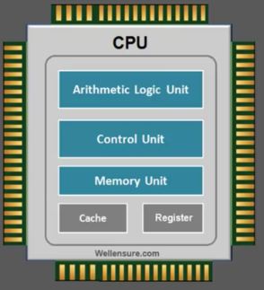
A CPU register is a high speed memory area built right inside the processor chip and a very imporatant component of the CPU design.
-
the CPU memory unit consist of different types of registers and each of these register perform a specific function during process execution.
-
the CPU register are closest and the fastest memory areas as a part of CPU’s internal memory. the CPU has different types of registers and each of these register perform a specific function.
-
the CPU registers are placed at the top of the memory hierachy and closest to the CPU. Register provide CPU, the fastest way to access data for a processor.
-
Register are normally measured by the number of bits they can hold. For example, a 8-bit register means it can store 8 bits of data or 32-bit register means it can store 32 bits of data.
-
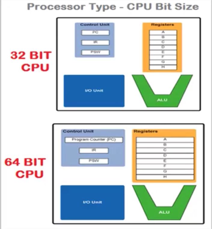
the number of register that a CPU has and the size of each register (number of bits) help determnine the power and speed of a CPU. for example a 32-bit CPU is one in which each register is 32 bits wide. therefore, each CPU instruction can manipulate 32 bits of data.
-
these registers are used to store the data temporarily during the program execution.
-
different processors can have different register size(16,32,64 bits) depending upon CPU architecture.
why register need?
-
the computer system memory unit consist of different types of memory arranged in hierarchical order depending upon the data access speed, distance from the CPU and size of the memory.
-
in computer system, a CPU register is a very high speed memory used to increase the execution speed of computer programs by providing quick access to the CPU to the frequecny used values.
-
every processor has this high speed local storage area known as a register that is used to holds the data which can be accessed by the ALU(arithmetic Logic Unit) which actually operates on this data as per the program instruction decoded by the CPU.
-
For ALU to perform any operation, the data must be first stored in a designated register where it can be manipulated by the processor.
-
For Example, to add two numbers in a arithmetic operation, the numbers are first stored in the registers as inputs where ALU performs arithmetic addtions and the results is sotred in another register.
-
the CPU register are divided in fi ve major categories depending upon the function assigned it and the visibility to the programmer:
- General Purpose Registers
- Pointer Registers
- Index Registers
- Segment Registers
- Flag Registers
-
A modern CPU consist of number of registers. each of these register has specific purpose and function associated with it.
-
there are number of general purpose registers that the programmer can use to hold intermediate results while executing the program instructions.
-
then there are special purpose registers designed to carry out a specific role. each of these registers are given a name so that the programmer can write their software code to access them. different manufactures of CPU chip call them by different names depending upon their function.
- User visible and modifiable
- General Purpose Register(GPR)
- Data Registers(Accumulator)
- Address Register(e.g base addressing, index addressing)
- Control Register(Not visible to the User)
- Program Conunter Register(PC )
- Current Instruction Register(CIR/IR)
- Memory Address Register (MAR)
- Memory Buffer Register(MBR/Memory data Register)
- state register(visible to user but not directly modifiable)
- Program status word register(PSW)
Functions of CPU Registers
-
all the data first must be represented in a corresponding CPU registers before it can be processed by the CPU. the CPU contains different types of memory register to handle different type of data and program instruction
- User visible and modifiable
- General Purpose Register(GPR)
- Data Registers(Accumulator)
- Address Register(e.g base addressing, index addressing)
- Control Register(Not visible to the User)
- Program Conunter Register(PC )
- Current Instruction Register(CIR/IR)
- Memory Address Register (MAR)
- Memory Buffer Register(MBR/Memory data Register)
- state register(visible to user but not directly modifiable)
- Program status word register(PSW)
- the MAR - Memory Address Register holds the address of memory where CPU wants to read or wirte the data. when CPU wants to store some data in the memory or reads the data from the memory, it places the address of the required memory loacation in the MAR register.
- MBR - Memory Buffer Register OR MDR -Memory Data Register
- when CPU performs instruction cycle the data or program instruction is fetched from memory and it is temporarily held in the MBR sometimes also called the Memory Data Register(MDR)
- A “buffer” is a commonly used computer term to describe memory designed to hold data that is on its way to somewhere else.
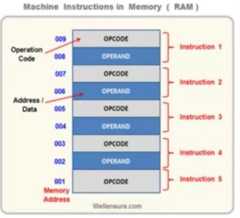
- the MBR/MDR contains the instruction and data retrived from the main memory which is than copied to the instruction register(IR) where the instruction is split inth the OpCode and Operand. the fetch part of the instruction cycle ends here. the Opcode is then decoded by the CPU decoder to perform the operation as program instruction.
-
insturction register : the contents MBR/MDR is transferred to a instruction register in CPU which holds the instruction to be executed by the CPU.
-
the instruction register breaks down the instrucion in two parts OPCODE and Operand. the OPCODE is interpreted by the CPU decoder as per the procssor’s instrucion set and the ALU - Arithmetic Logic Unit perform the operation on the operand (data/address). the result of this operation is temporarily stored in accumulator register.
-
Accumulator Registor
- in CPU, an accumulator is a register in which intermediate arithmetic and logic results are stored during execution of instruction cycel and subsequently transferred to main memory RAM.
- the result of this operation performed by the ALU is temporarily stored in accumulator register. without a register like an accumulator, it would be necessary to write the result of each calculation(such as addition, multiplication) to the main memory RAM.


